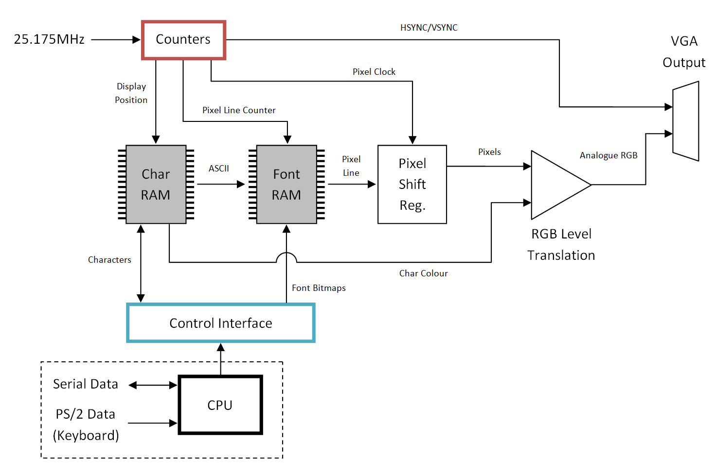
The block diagram below gives an overview of how the terminal works:
The following sections describe the logic on each page of the schematics. Click the PDF icon next to the title to open the relevant schematic in a new tab.
A 25.175MHz oscillator clocks a counter which provides the horizontal address and HSYNC video timing pulses. A second counter clocked from HSYNC provides the vertical address and VSYNC timing pulses. The timing and pulse polarity is for a 640x480 VGA signal at 60Hz. Monitors recognise the timing of the pulses as VGA resolution.
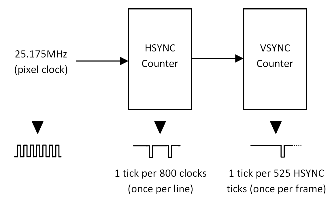
The horizontal address counter is made up of three chained 4-bit synchronous counters [U1, U2 & U3] making a 12-bit counter, of which only 10 bits are used for the horizontal address bits (HA0-HA9). These are used as RAM addresses to scan a line of characters. The count increments with each tick of the pixel clock from XOSC1. When the count reaches 799, the output of U4B (nRST799) goes low causing the counter to be reset on the 800th clock (the counter RST input is synchronous). The value 799 in binary is 11 0001 1111. Pin 15 of U1 (terminal count) goes high when U1's count is 1111 and this is AND'ed with U2 pin 14 (HA4) by U5A. The top two bits of the 799 pattern coming from U3 (HA8 & HA9) are AND'ed with the lower bits by U4B and inverted.
The vertical address counter works in much the same way as the horizontal counter, but is clocked by the HSYNC pulse so it increments once per line (each time the horizontal counter is reset). Because the vertical counter is running 800 times slower than the horizontal counter, we can use a more integrated device [U6] which is a 12-bit asynchronous (ripple) counter. The downside of ripple counters is their outputs take much longer to settle to the correct count value but this instability occurs at the start of each line, before the visible part of the scan. The vertical count resets every 525 clocks. We could have used gates to decode a count of 525 and connected that to the RST input but this would have resulted in a glitch on the reset input and the same signal is used to generate the VSYNC pulse, so instead, we decode 524 (binary 10 0000 1100) with U7A and clock this through to the counter RST on the next HSYNC clock using a flip-flop [U8A]. In effect, we have made U6's RST input synchronous. The count outputs from U6 form the vertical address (VA0-VA9) and are used as address inputs to the character RAM in a similar way to he horizontal address bits.
The horizontal sync pulse is synchronous with the pixel clock and is generated by a flip-flop [U9A]. The flip-flop has a '0' clocked in when the horizontal counter resets (nRST799 low forces U5B output low). The inverted output of U9A is fed back to an AND gate [U4C]. Since the counter has just been reset, the signal nHSYNC95 is high and the low output from U4C keeps the D input of U9A low after nRST799 has gone high due to the counter reset. This state perists until nHSYNC95 goes low when the count reaches 95. At this point the D input of U9A becomes high and, on the next rising edge of PIXCLK, HSYNC goes high. In total, HSYNC goes low for 96 pixel clocks with the falling edge coincident with the HSYNC counter resetting. In this simple design, the front/back porches and blanking are a property of the character positions in the RAM (see explanation later).
The vertical sync pulse is generated by a flip-flop [U8B]. When the vertical count resets, signal RST525 goes high on the rising edge of HSYNC, the inverted output of U8A clears the flip-flop [U8B] and VSYNC goes low. The CLR signal is low for a whole line. On the next line CLR is released on the rising edge of HSYNC and a '1' is clocked in on the next falling edge of HSYNC so VSYNC is low for 2 line periods minus the width of HSYNC (96 clocks) or about 59.75µs.
Monitor power save is accomplished by turning off both sync signals. When the nSLEEP signal is set low by the CPU, HSYNC and VSYNC are driven high and the horizontal counter is reset by loading zero's on the parallel inputs P0-P3. The vertical counter is also reset. In this state the crystal oscillator is still running, as is the CPU, but almost everything else on the board has stopped. Terminal power consumption drops from about 0.5W (100mA) to 0.25W (50mA) and the monitor turns off the screen, typically saving hundreds of Watts. The PIC software can automatically enter sleep mode after a certain time if required (see setup screen) and an escape sequence can be sent to enter power save mode. Received characters or keyboard key presses wake up the terminal with no loss of data.
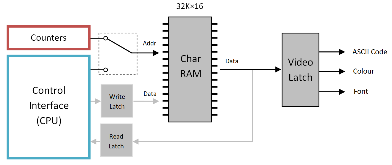
There are two character RAM chips [U27 & U28] (each 8 bit wide, accessed as a single 16-bit wide RAM) which store the character information for each position on the display. U27 contains the ASCII code of the character while U28 contains the colour and font information.
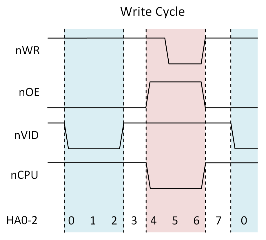
Access to the character RAM alternates between the CPU and video scan circuitry. While the video only reads the RAM, the CPU has read and write access to any random address. During the first half of each byte cycle (8 pixel clocks), the video circuitry has access to the character RAM and during the second half the CPU has access. The RAMs are fast enough to complete a single read or write access in half a byte cycle. The following diagrams illustrate the active parts of the circuit for each access type.
Video Read Cycle
The video circuits can only read the RAM - the address comes from the counters through the 'video address buffer' [U25 & U26] and the data is latched by the 'video data read buffer' [U23 & U24].
CPU Read Cycle
The CPU reads the RAM by loading the 'CPU address buffer' [U10 & U11] and reading from the 'CPU data read buffer' [U12 & U13].
CPU Write Cycle
The CPU writes to the RAM by loading the 'CPU address buffer' [U10 & U11] and 'CPU data write buffer' [U14 & U15] and toggling the WREQ signal to U21B.
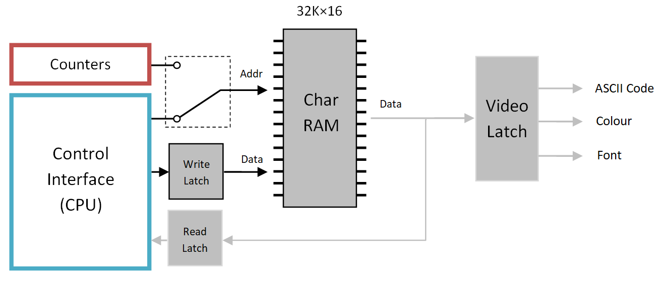
The horizontal and vertical counts (HA0-9 and VA0-9) are very important signals which are used throughout the circuit as RAM addresses, as control signals to share the RAMs with the CPU and to generate the RAM read/write control signals. It is worth pausing at this point to explain what address goes where and why...
Detailed RAM timing The diagrams below show the nVID, nCPU, nOE and nWR signals over one byte cycle (8 pixel clocks, about 318ns). The two active-low signals nVID and nCPU enable the video and CPU access buffers shown in the diagrams above. During the blue period, the character RAM is read for the video scan and during the red period the CPU has access to the RAM, allowing 159ns for each read or write to complete. Between each access there is a [white] gap where no buffers are enabled. This is to prevent overlaps where two buffers are enabled at the same time due to timing differences.
In the diagrams, the first dotted line is the start of a timing cycle, the video read is active in periods 0, 1 and 2, then there is a one period gap followed by the CPU read/write in periods 4, 5 and 6 and a final gap. The diagram on the left shows a CPU read cycle and the one on the right shows a CPU write cycle.
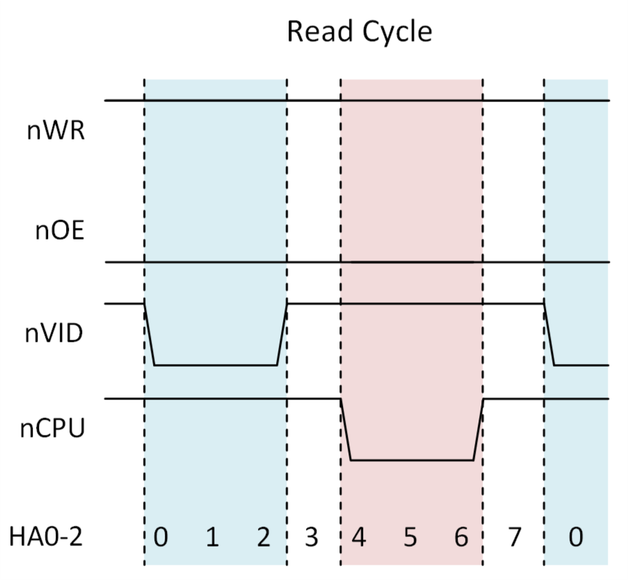
These signals are generated by the circuit marked 'RAM Timing Generation' on the schematic. U18 decodes the pixel count (HA0-2) into 8 time periods of just less than 40ns each when outputs Y0-Y7 go low in turn. The gates select the periods of interest and U22 re-times the signals (one clock delayed) to make clean synchronous signals. For example, nVID is the AND of Y0, Y1 and Y7 - that means that the output of U7B will be low if any of those signals are low. In other words, the output of U7B will be low in time periods 7, 0 and 1, but U22 will re-time the signal so it is low one clock later i.e. in period 0, 1 and 2 as shown in the diagram above.
The RAM output enable [nOE] signal is normally kept low and only goes high during a write cycle, when it goes high one cycle before nWR goes low to give time for the RAM to release the data bus before we start driving it [with U14 & U15]. nWR is active (low) for 2 cycles (about 80ns) which is plenty of time to meet the RAM's 55ns access time requirement.
The two flip-flops [U21] are used to perform CPU writes to the RAM. The output of U21B goes high on the rising edge of WREQ - it doesn't matter how long the CPU takes to bring WREQ low again as the flip-flop is only sensitive to the rising edge. The output is sychronised to the pixel clock by two trips through U22 to prevent metastability. The signal is presented to the D input of U21A where the request is recognised at the start of the next timing cycle (the rising edge of nY7). U21's inverted output ensures that the next CPU cycle is a write request and the request is cancelled when nY6 goes low at the end of the write cycle (nWR goes high one pixel clock later).
In the worst case, a write cycle takes two byte cycles plus two pixel clocks i.e. 18 clocks = 720ns. This is because the request has to be synchronised to PIXCLK in U22, then if a cycle has just started, it will be 8 clocks before a cycle starts, then the next cycle is required to complete the write. In the worst case a read requires one and a half cycles (a request could come half way through the cycle but too late to be valid in the current cycle, then it takes one more cycle to see the result - for a total of 480ns) so the CPU read/write memory bandwidth is >1.3MHz. In practice the bottleneck is the (PIC) CPU performance, though an alternative CPU or a hardware implementation could potentially outrun the RAM.
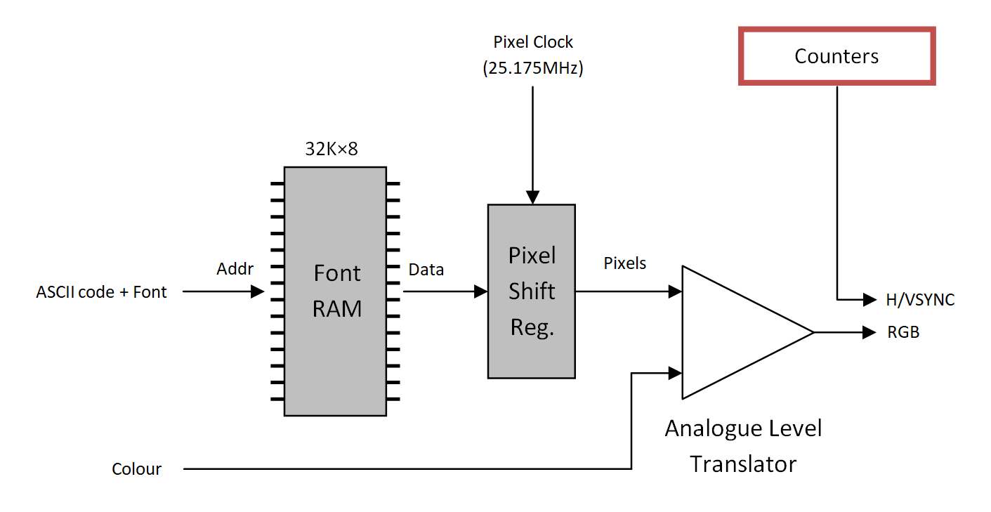
nY0 and nY7 (the first and last period) are also used by the pixel output logic [U30 & U31] to load the pixel output shift register and colour latch so the pixels emerge at the correct time with the correct colour.
The signal nFOE (font RAM output enable, active low) is used to assert nWR when loading the font RAM (see font RAM description). During this procedure the video output is blanked and the character RAMs are disabled [nCHAR is high] so no actual writes occur to the char RAM and the state of nOE is also irrelevant.
The font RAM stores the bitmap images for each of the characters in each of the fonts. The character for the current screen position is loaded from the character RAM and is used as the address for the font RAM read. A single horizontal line of the character, 8 pixels wide, is then put into the pixel shift register, which outputs the pixels to the display at the pixel clock rate (25.175MHz).
In this design a single character cannot have more than one colour e.g. if "ABC" is displayed, each character A, B or C can be a different colour but 'A' cannot be a mixture of colours. Each character is actually 2 colours where one is black e.g. red on black or black on yellow. Inside the Font RAM the coloured bit is a '1' and the black bit is a '0'. Within the character all the '1' pixels are the same colour so you can't have an 'A' displayed where the left half is green and the right half blue. This is because the character colour is stored in the character RAM which is only read one byte at a time and the colour persists for the next 8 pixels. The colour information is mixed with the pixel information before going into the analogue level translator to generate the R, G and B video signals.
The HSYNC and VSYNC signals are generated by the counters and go directly to the VGA output, along with the now analogue RGB levels.
Circuit Operation The circuit is normally in 'Display Mode' but can be powered down (which also turns the monitor off) or put in a special mode to load the Font RAM which occurs on power up and whenever a new custom character is set.
| nSLEEP | nCHAR | nFOE | nFWR | Mode | Description |
|---|---|---|---|---|---|
| 0 | 1 | 0 | 1 | Power Down Mode | H/VSYNC high, H/V counters stopped, display is blanked. |
| 1 | 0 | 0 | 1 | Display Mode | Char RAM and Font RAM are both enabled. Font RAM is read-only. |
| 1 | 1 | 0 | 1 | Font Load Mode | Char RAM is disabled. Font RAM addr FA0-3 set by CPU, display is blanked. |
| 1 | 1 | Pulse High | Pulse Low | Font RAM Write Cycle | CPU sets nFOE high, then nFWR low, data in U17 is written. |
| One Byte | ||||||||
| 0x0 | ||||||||
| 0x1 | ||||||||
| 0x2 | ||||||||
| 0x3 | ||||||||
| 0x4 | ||||||||
| 0x5 | ||||||||
| 0x6 | ||||||||
| 0x7 | ||||||||
| 0x8 | ||||||||
| 0x9 | ||||||||
| 0xA | ||||||||
| 0xB | ||||||||
| 0xC | ||||||||
| 0xD | ||||||||
| 0xE | ||||||||
| 0xF | ||||||||
| <- 256 chars (4K) -> | ||||
| G0 (16K) |
0x00 | 0x01 | 0x02 | ... |
| Reverse Vid | ||||
| Underlined | ||||
| UL + Rev | ||||
| G1 (16K) |
. . . |
|||
| PIXELS | BRI | Transistor Base | RGB Signals |
|---|---|---|---|
| 0 | 0 | 0V | 0V |
| 0 | 1 | * | * |
| 1 | 0 | 1.05V | 0.35V |
| 1 | 1 | 1.4V | 0.7V |
The CPU [U34] controls the operation of the terminal, see the Software page for more information.
J6 is a standard PIC header used to program and debug the CPU. Pin 4 is shared with the RTS signal. When the flow control setting is RTS/CTS, the CPU can no longer be programmed or debugged as the debugger cannot control the CPU. To re-program the CPU or use the debugger, the flow control setting must first be set to None or XON/XOFF.
If you want to replace the CPU with your own control circuit, you will have to interface via the following GPIO signals:
The RS232 driver [U35] takes a serial data connection from a 9-way D-connector [J3] and converts it to logic level for input into the CPU. The 9-way D-connector can be bypassed by disconnecting jumper JP1 and instead plugging a 5-way serial connector into J2. Power for the terminal can also be supplied via J2, so for a logic level UART connection, only one connector is required.
In the schematic, the RS232 driver chip is shown as a MAX232E, however this part can be quite expensive and requires high value capacitors [C3-7] (~10µF), so a pin compatible driver can be put in its place to cut the cost. The downside of this is that a MAX232E will run at 230kbaud, whereas cheaper equivalents will only run at a maximum of 115kbaud.
The keyboard input is a standard female PS/2 connector [J5] that connects to the CPU. It also has some supplementary components that provide basic filtering for the signals [R2/3, C43/44]. The CPU interprets the keyboard input and transmits the keystrokes on the serial line as ASCII characters.
The 5V power in this circuit can be supplied from two different sources. Normally from a 2.1mm jack [J1], but alternatively through the serial connector [J2].
The 5V power goes through a fuse [F1] and power LED [D2]. Diode D1 acts as reverse voltage protection, effectively shorting the power rails together and blowing fuse [F1] if the power is connected in reverse.
Capacitors [C1/2] are bulk decoupling capacitors and can be found on opposite corners of the PCB. Capacitors [C8-42] are decoupling capacitors for each of the devices on the PCB, and can be found close to each device.